All Facilities | All Instruments
Nanofabrication Facility
Instruments and Tools
Metrology
-
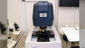
3D Optical Profiler ›
The Bruker Contour GT-I is a fully automated and programmable optical interferometric microscope that can be used to measure and map surface features in 3D.
-
Atomic Force Microscope (AFM) ›
The Bruker Dimension FastScan AFM provides high speed topographic imaging without loss of resolution or force control.
-
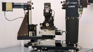
Ellipsometer ›
The Woollam V-VASE is a Variable Angle Spectroscopic Ellipsometer capable of automated thin-film characterization, high-precision angle, and a wide spectral range (240 nm to 2500 nm).
-
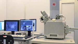
Field Emission Scanning Electron Microscope (FE-SEM) ›
The FEI Nova NanoSEM™ is a high resolution scanning electron microscope intended for sample characterization.
-
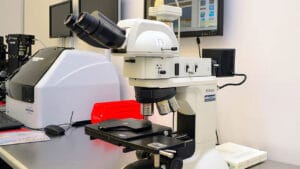
Inspection Microscopes ›
The system of Nikon Eclipse Inspection Microscopes has a 6”x6” stage and is configured with bright-field, dark-field, and simple polarizing objectives.
-
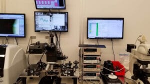
Probe Station ›
The probe station is equipped with two Keithley 2400 Source Meters, a Keithley 6485 picoammeter, and a Keithley 2000 Diginal Multimeter.
-
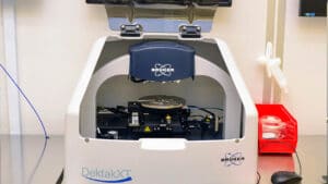
Stylus Profiler ›
The Bruker Dektak-XT is a semi-automated stylus profiler that can be used to measure step height with better than 5 Å repeatability, surface roughness, as well as 3D surface mapping.
-
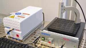
Thin Film Analyzer ›
The Filmetrics F20 is used to measure the thickness and optical constants (n and k) of transparent and semi-transparent thin films.


