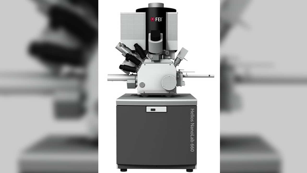
FEI Helios Nanolab 660 FIB-SEM

The FEI Helios NanoLab 660 features the most recent advances in field emission SEM (FESEM) and focused ion beam (FIB) technologies and their combined use. This DualBeam SEM/FIB is designed for demanding nanoscale work, resolving the finest details (extremely high resolution) in 2D and 3D with clearest contrast, nanoprototyping, and highest quality sample preparation.
The Helios NanoLab 660 is a highly flexible platform for high productivity TEM sample preparation and high performance imaging. It is designed to deliver multi-scale, multi-dimensional insights, and down to sub-nm resolution. The combination of automated sequential focused ion beam (FIB) milling and scanning electron microscope (SEM) imaging allow for collection of a series of 2D images, which leads to 3D volume reconstructions. The attached Oxford EDX detector provides elemental and chemical analysis that gathers accurate data at the micro- and nanoscales.
Features
- Elstar electron gun with Schottky thermal field emitter
- ConstantPower™ lens technology for higher thermal stability
- Probe current:
- E-beam: 0.8 pA – 100 nA
- I-beam: 0.1 pA – 65 nA
- Electron beam resolution at optimum WD:
- 0.6 nm from 15 kV to 2 kV
- 0.7 nm at 1 kV
- 1.0 nm at 500 V
- Electron beam resolution at coincident point:
- 0.6 nm at 15 kV
- 0.9 nm at 5 kV
- 1.2 nm at 1 kV
- Ion beam resolution at coincident point:
- 2.5 nm at 30 kV
- E- and I-beam coincidence point at analytical WD (4 mm SEM)
- Landing voltage range
- E-beam: 20 V – 30 kV
- I-beam: 500 V – 30 kV
- High precision 5-axes motorized stage
- Detectors
- Elstar in-lens SE detector (TLD-SE)
- Elstar in-lens BSE detector (TLD-BSE)
- Elstar in-column BSE detector (ICD)
- Elstar in-column BSE detector (MD)
- Everhart-Thornley SE detector (ETD)
- IR camera for viewing sample/column
- In-chamber sample navigation camera (Nav-Cam)
- Retractable low voltage, high contrast solid-state backscatter electron detector (CBS)
- Retractable STEM detector with BF/DF/HAADF segments
- High performance Ion Conversion and Electron (ICE) detector for secondary ions (SI) and electrons (SE)
- Dwell time range from 0.025 to 25,000 μs/pixel
- Up to 6144 ~ 4096 pixels
- GIS – beam chemistry option: Platinum deposition
- Manipulator: Easylift for thin TEM sample preparation
- Oxford EDX detector for energy-dispersive X-ray spectroscopy (EDS)
- Integrated plasma cleaner
- High-resolution multi-stub mount holder
Software
- Auto Slice & View G3 for automating the acquisition of high-resolution 2D image stacks. It acquires data by milling serial sections (slices) and then imaging each slice of a user-defined volume of the sample. This software enables study of the 3D structure and composition of samples at the nanometer scale.
- MAPS for automated acquisition of high resolution images from large areas.
- FEI NanoBuilder for systematic planning of construction of multi-layer nanostructures by dividing CAD files into ordered projects.
- Aztec for EDS data collection and analysis
- Avizo, Amira: advanced 3D analysis softwares for straightforward visualization and measurement to advanced image processing, quantification, analysis and reporting.
Contacts
- Sheng Zhang, Ph.D.
Electron Microscopy Specialist, Imaging Facility
[email protected]
Manufacturer / Model
Thermo Fisher Scientific (former FEI) / Helios NanoLab 660
Facility
Imaging Facility
Keywords
auto slice & view, energy-dispersive X-ray spectroscopy (EDS), focused ion beam (FIB), microscope, scanning electron microscope (SEM)
